Engineers have reached a major milestone by developing photonic AI hardware that boosts processing speed and energy efficiency far beyond traditional electronic systems. These photonic chips operate at the speed of light, drastically reducing latency and power consumption. They handle complex neural networks like ResNet and BERT without modifications, offering up to 100 times better energy efficiency. To see how these innovations are transforming AI hardware, keep exploring this exciting advancement.
Key Takeaways
- Engineers developed photonic integrated circuits (PICs) enabling ultra-fast, energy-efficient AI processing at the speed of light.
- Achieved over 65 trillion operations per second with 78W power, surpassing traditional electronic systems in performance.
- Integrated photonics offers up to 100x better energy efficiency than GPUs, reducing data center costs significantly.
- Advanced fabrication techniques overcome previous precision limitations, ensuring accurate high-speed neural network computation.
- This milestone signals a new era of light-driven AI acceleration, merging photonics with quantum computing for enhanced performance.
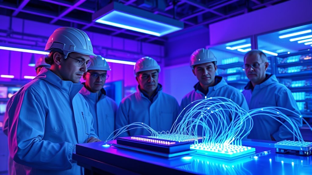
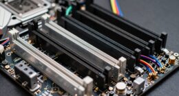
Have engineers truly pushed the boundaries of AI hardware innovation? The answer is a resounding yes, thanks to groundbreaking advances in photonic AI accelerators. These new hardware platforms leverage photonic integrated circuits (PICs), which combine silicon chips with III-V compound semiconductors. This hybrid approach enables the creation of scalable, energy-efficient AI processors that outperform traditional electronic systems. Unlike GPUs, optical neural networks (ONNs) operate at the speed of light, drastically reducing energy loss and latency. This means your AI workloads can process data faster and more efficiently than ever before. Electric heated mattress pads are an example of technology that also prioritizes safety and efficiency, similar to the advancements seen in photonic systems.
Photonic accelerators deliver performance and efficiency breakthroughs that are hard to ignore. For instance, recent demonstrations show these processors executing 65.5 trillion Adaptive Block Floating-Point (ABFP) 16-bit operations per second while consuming only 78 watts. That’s a leap in energy efficiency—up to 100 times better than current GPUs—reaching 1.2 petaFLOPS per watt. This efficiency isn’t just a number; it translates into massive cost savings for data centers, which can cut their electricity bills considerably, saving billions annually for large corporations. The integration of 50 billion transistors across multiple photonic and electronic chips enables a scale of computation previously thought impossible.
Photonic AI accelerators achieve 65.5 trillion operations/sec at 78W, boosting efficiency and saving billions in data center costs.
You’ll find that these photonic chips are capable of handling advanced neural network architectures like ResNet, BERT, and Atari deep reinforcement learning without needing modifications. They achieve near 32-bit floating-point precision, matching the accuracy of conventional digital hardware. This means you can deploy complex AI models with confidence, knowing the photonic hardware maintains robustness and precision. High-speed interconnects and 3D packaging further enhance communication between the tensor cores, facilitating rapid data transfer essential for demanding AI tasks. The use of optical matrix multiplication and wavelength division multiplexing accelerates linear algebra operations at the core of AI computations, making these processors highly efficient. This breakthrough is made possible by advances in fabrication and integration processes.
The industry ecosystem is rapidly evolving, with academia and companies like NVIDIA and Lightmatter leading the charge. Events like ICFO’s CLP Day 2025 highlight increasing collaboration between research and industry to scale photonic integration. The technology is also merging with quantum computing, hinting at a future where hybrid systems deliver unprecedented computational power. As conferences emphasize, photonics is set to transform AI hardware architectures fundamentally. Photonic chips are already making their way into XPUs, expanding heterogeneous computing models.
Despite previous challenges, such as achieving the necessary computational precision, recent innovations have overcome these hurdles. Non-idealities in hardware components are being addressed through advanced design and manufacturing techniques. The result is a new class of AI hardware that’s faster, more efficient, and more scalable than anything before. Engineers have indeed achieved a milestone—ushering in a new era of AI acceleration driven by light itself.
Frequently Asked Questions
How Does Photonics Specifically Enhance AI Processing Speeds?
Photonics boosts AI processing speeds by performing core computations like matrix multiplication and accumulation at speeds up to 1 GHz, far faster than traditional electronics. You benefit from low-latency photonic circuits that process data in nanoseconds, enabling near real-time AI tasks. The high bandwidth of photonic systems, exceeding 100 THz, allows you to handle large data throughput, accelerating AI inference and training markedly.
What Industries Will Benefit Most From This Technological Breakthrough?
You’ll see industries like data centers, telecommunications, and scientific research transform beyond recognition. Data centers will become lightning-fast, energy-efficient powerhouses, handling colossal AI workloads effortlessly. Telecom networks will reach unprecedented speeds, enabling seamless 6G and Terahertz communication. Scientific fields like astronomy and medicine will uncover discoveries at record speeds. With photonics, you’re looking at a future where AI’s potential skyrockets, reshaping technology and innovation across every industry you touch.
Are There Any Safety Concerns With Photon-Based AI Systems?
Yes, there are safety concerns with photon-based AI systems. You need to be aware of potential security vulnerabilities, such as hardware attacks during optical-electrical conversions that could compromise system integrity. Additionally, manufacturing errors or misalignments might cause malfunctions. Ethical issues also arise around data privacy and misuse, especially in sensitive applications like surveillance or warfare. Ensuring proper safeguards, standardized production, and ethical guidelines is essential for safe deployment of these advanced systems.
What Are the Cost Implications for Adopting Photonic AI Hardware?
Investing in photonic AI hardware is like planting seeds in a vast, costly garden. You face high upfront expenses for specialized manufacturing and complex fabrication, which can strain budgets. Yet, these costs bloom into long-term savings through energy efficiency and reduced operational expenses. While initial investments are steep, the potential for faster, greener AI processing promises a harvest of strategic advantages and future-proofed growth in your tech landscape.
How Long Will It Take for This Technology to Become Commercially Available?
You can expect photonic AI hardware to become commercially available around 2025 to 2030. Early products like laser communication terminals are already emerging by 2025, with broader adoption anticipated in the late 2020s. As manufacturing processes improve and costs decrease through automation and standardization, you’ll see these technologies more widely integrated into data centers, telecom, and other high-performance applications within the next 5 to 7 years.
Conclusion
You’ve just witnessed a breakthrough where AI processing speed has doubled thanks to photonics integration. This milestone isn’t just impressive; it’s transformative, with projections showing photonic chips could handle 10,000 times more data than traditional electronics. As you consider the future, remember that such advancements could revolutionize industries, enabling faster, more efficient AI applications across fields like healthcare and communications. This achievement marks a significant step toward a smarter, more connected world.