
Semiconductors are the core materials in microchips, enabling devices to process and store information. They can switch between conducting and insulating states, which makes them essential for transistors and circuits. During manufacturing, precise doping introduces impurities to control electrical properties. Advances in nanotechnology and quantum tunneling are pushing smaller, faster devices to their limits. If you explore further, you’ll discover how these materials shape modern technology and what’s next in semiconductor innovation.
Key Takeaways
- Semiconductors are materials that can switch between conducting and insulating states, forming the foundation of microchips.
- Manufacturing involves doping processes that introduce impurities to control electrical properties of silicon.
- Quantum tunneling at nanoscale features affects device performance by causing leakage currents.
- Microchip fabrication uses advanced nanotechnology for precise impurity placement and miniaturization.
- These combined processes enable the creation of faster, smaller, and more efficient electronic devices.

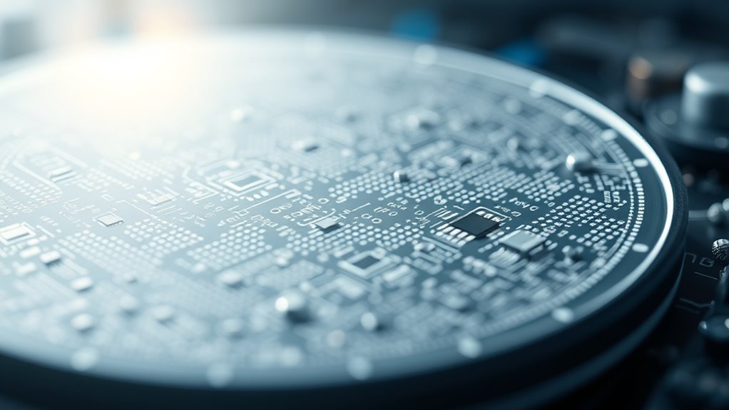
Have you ever wondered what makes your smartphones, computers, and countless electronic devices work? At the heart of these gadgets are semiconductors—materials that can switch between conducting electricity like metals and insulating like plastics. Understanding how semiconductors operate starts with grasping some key concepts, such as quantum tunneling and doping processes. These phenomena are fundamental to how microchips function and how manufacturers create the tiny, powerful components you rely on daily.
Quantum tunneling is a fascinating quantum mechanical effect that occurs when particles, like electrons, pass through barriers that classical physics would deem impenetrable. In semiconductors, this effect becomes significant as device features shrink to nanometer scales. When electrons encounter potential barriers within a tiny transistor, instead of bouncing back, they sometimes tunnel through, enabling current flow even when traditional conduction isn’t possible. This process is both a challenge and an opportunity. On one hand, it can cause leakage currents that affect device efficiency; on the other, engineers harness quantum tunneling to develop faster, smaller transistors that push the limits of technology. As device dimensions continue to decrease, understanding and controlling quantum tunneling is vital for maintaining performance and power efficiency in modern microchips.
Quantum tunneling enables electrons to pass through barriers, driving smaller, faster, and more efficient semiconductor devices.
Doping processes are another cornerstone of semiconductor technology. Doping involves intentionally introducing impurities into a pure semiconductor material—usually silicon—to modify its electrical properties. By adding elements like phosphorus or boron, you can create regions rich in free electrons (n-type) or holes (p-type), which are essential for building transistors, diodes, and integrated circuits. These doped regions form the basic building blocks of microchips, allowing them to switch states rapidly and reliably. The precise control over doping concentrations and locations during manufacturing ensures that transistors can toggle between on and off states, enabling digital logic and memory functions. The doping process is highly refined; it involves techniques such as diffusion or ion implantation, which deposit impurities into silicon wafers with extreme accuracy. This meticulous process results in the complex circuitry inside your devices that perform computations, store data, and communicate with other components.
Additionally, advances in nanotechnology have further enhanced our ability to manipulate quantum effects and doping at atomic scales, leading to even more miniaturized and efficient microchips. In essence, the operation of semiconductors hinges on controlling electron behavior at the quantum level and manipulating the material’s properties through doping. Quantum tunneling influences how small transistors behave and what limits their miniaturization, while doping processes set the stage for creating the semiconductor’s electrical characteristics. Together, these phenomena enable the microchips that power your digital world, transforming raw materials into sophisticated electronic systems. By understanding these fundamental principles, you gain insight into the intricate science behind the devices you use every day and appreciate the remarkable engineering that makes modern technology possible.
Frequently Asked Questions
How Do Semiconductors Differ From Insulators and Conductors?
You’ll find that semiconductors differ from insulators and conductors in their electrical conductivity, which is moderate compared to the high conductivity of conductors and low conductivity of insulators. As a material classification, semiconductors can switch between conducting and insulating states based on conditions like doping or temperature. This unique ability makes them essential for microchips, allowing precise control over electrical flow in electronic devices.
What Are the Environmental Impacts of Semiconductor Manufacturing?
You should know that semiconductor manufacturing impacts the environment through high energy consumption and water pollution. The process requires significant energy, often from non-renewable sources, contributing to greenhouse gases. Additionally, water pollution can occur from chemicals used during fabrication, which may contaminate local water supplies if not properly managed. To minimize these impacts, many companies are adopting greener practices and improving waste management techniques.
How Do Different Doping Elements Affect Semiconductor Properties?
Think of doping elements as the secret ingredients that spice up your semiconductor’s performance. Different doping elements, like boron or phosphorus, influence the semiconductor’s conductivity by creating either holes or extra electrons—this is doping element effects. You control impurity levels carefully to guarantee peak function, making impurity control vital. By choosing the right doping elements, you tailor your microchip’s electrical properties for specific applications, enhancing efficiency and performance.
What Are the Latest Advancements in Semiconductor Fabrication Technology?
You’ll find that the latest advancements in semiconductor fabrication include advanced lithography techniques like extreme ultraviolet (EUV) that enable smaller, more precise features. Additionally, 3D integration allows for stacking chips vertically, boosting performance and reducing size. These innovations help you develop faster, more energy-efficient microchips, meeting the demands of modern electronics. Staying updated on these trends guarantees you leverage cutting-edge technology to create the next generation of microdevices.
How Is Semiconductor Supply Chain Affected by Global Geopolitical Issues?
Imagine a delicate spiderweb trembling with the slightest breeze—that’s your semiconductor supply chain under global geopolitical tensions. When countries face conflicts or sanctions, supply chain disruptions occur, making it harder to source raw materials and advanced equipment. This causes delays and shortages, impacting everything from smartphones to cars. You might find yourself waiting longer for tech products or paying higher prices, as geopolitical issues send shockwaves through the semiconductor industry.
Conclusion
Now that you understand the basics of semiconductors and how microchips are made, you see their essential role in modern technology. From smartphones to computers, they power everything around us. Isn’t it amazing how tiny chips have such a huge impact? By grasping these fundamentals, you’re better equipped to appreciate the complex world of electronics. So, next time you use a device, remember the tiny semiconductor working behind the scenes.